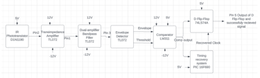
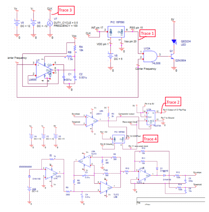
ASK IR Transceiver/Receiver
A basic digital communication system that utilizes amplitude shift keying
This was a project for a communication systems course, to apply the concepts learned in class. Overall, with all the parts integrated and tested, the transmitter and receiver circuit properly sent and received the pseudorandom bit sequence without errors, up to a distance of 32 inches between the two breadboards. Even the recovered bit clock on the receiver circuit is extremely accurate, where the D Flip-Flop can receive accurate bits up to 3.9kHz clock speed.
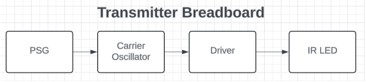
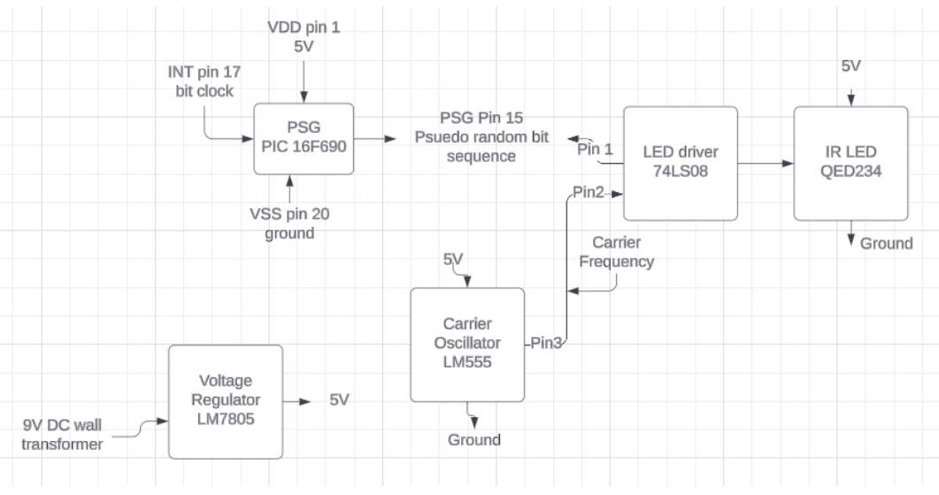
On the Transmitter Breadboard:
The PSG subsystem provides a pseudorandom bit sequence, which is meant to mimic a random signal to be sent, which will then be transmitted to the receiver circuit. This system takes in a bit clock on how fast to send bits and connects to the carrier oscillator subsystem. For the receiver breadboard to appropriately receive the bits with no error, the system bit clock needs to be under 3.9 kHz. The other inputs to the PSG include 5V for power and a ground pin, and the output is the pseudorandom bit sequence.
The PSG then leads in the carrier oscillator to modulate the signal at 40 kHz so the signal is transmitted correctly. The 40 kHz carrier oscillator is designed using a LM555 timer and uses resistor values to generate a 50% duty cycle. The PSG output and the 40 kHz carrier are then provided as input to an AND gate to drive the LED, so the signal is transmitted through the phototransistor.
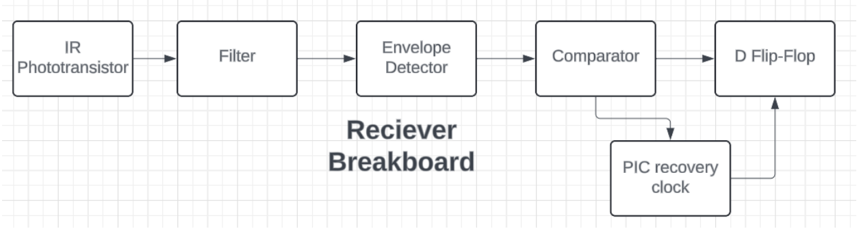
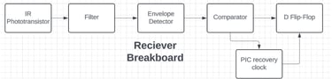
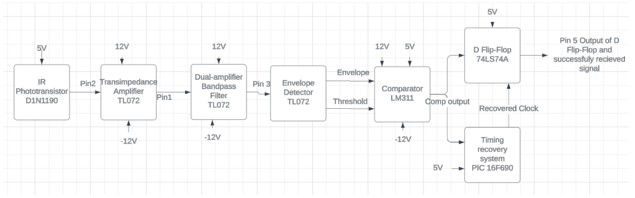
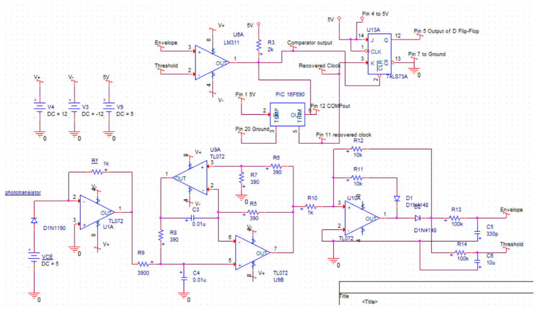
On the Receiver Breadboard:
The transmitted signal is received by the IR phototransistor receiver powered by a 5V driver. This received signal is then passed through a Dual-Amplifier Bandpass Filter to eliminate most of the 40kHz carrier frequency in the signal. A positive and negative 12-volt source is needed to power the two TL072 amplifiers, and the parameters of the filter include having a center frequency of 40 kHz with no more than an error of 5%, a 3db bandwidth of 5 kHz, and a midband gain of about 2.8.
After the filter, the signal is passed through an envelope detector to get an envelope of the signal and a threshold. The first stage of the envelope comprises an op-amp and diodes, which function as a half-wave rectifier. The second stage is a simple low-pass filter that is less than the carrier frequency of the envelope detector but large enough to pass the envelope. Creating a 5 kHz low-pass filter works great for these requirements. The third state is also a low-pass filter that only passes the DC value of the envelope pass. A low-pass filter of less than 100 Hz but greater than 10 Hz effectively passes the threshold. The half-wave rectifier inverts the signal and changes all positive values of the signal to zero to make the signal similar to the output of the PSG. The output of the envelope detector is the envelope of the signal and the threshold value.
The envelope and threshold value outputs then go into the comparator to clean up the envelope to eliminate any noise and error. The voltage comparator used is an LM31.1, which is powered by a 5V supply and alongside positive and negative 12V rails. The output of the comparator is a delayed copy of the pseudorandom signal produced by the PSG on the transmitter breadboard.
To store the correctly received signal, a D Flip-Flop is used. However, to store the value at the correct data rate, the Flip-Flop needs to be clocked by the transmitter bit clock. This bit clock is recovered by programming a PIC16F690 to take the input of the output of the comparator and generate a recovery clock for the D Flip-Flop. As stated before on the transmitter breadboard, the system bit clock needs to be under 3.9 kHz for the D Flip-Flop to store all the correct bits of the received signal properly. Like the previous PIC, a 5V supply also powers the timing recovery PIC. Finally, the value stored in the D Flip-Flop is the recovered signal transmitted and should be a perfect copy of the PSG output, but is delayed by half a period due to when the Flip-Flop is clocked to store its value.

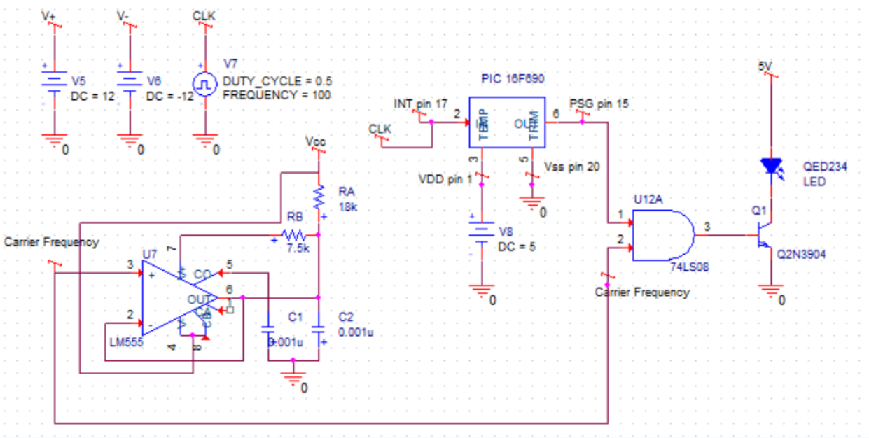
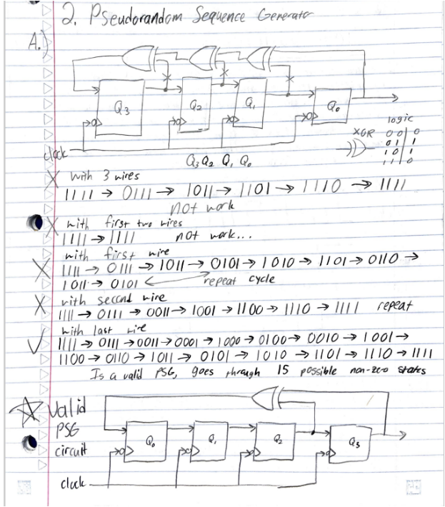
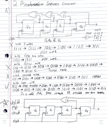
The PSG PIC has 16 Shift registers and is coded to have 65535 possible non-zero states, where it can run for a period of 655.35 seconds, given a frequency of 100Hz. To the right is a logic diagram of a simplified version of the pseudorandom circuit with fewer D Flip-Flops. The idea is to cycle through every possible non-zero state to generate a pseudorandom sequence to output. As the register is clocked, it will cycle through a sequence of states and periodically return to the original state once done with the entire period.
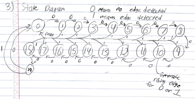
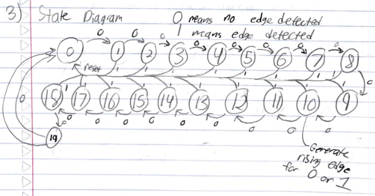
The second PIC is programmed to be a timing recovery system where it generates a clock that runs at 20 times the frequency that is wanted and then uses a counter clocked at this 20x rate to divide the frequency down to the clock rate of the transmitter. Thus, the counter is designed to reset whenever it detects an edge in the received data stream and also trigger the sampling D flip-flop in the receiver whenever the count reaches ten. If there are no edges in the received data stream, the counter wraps around from nineteen to zero and generates another edge once the count returns to ten, as shown in the state diagram to the right.
Logic Diagram of Simplified PSG
State Diagram of the Timing Recovery System
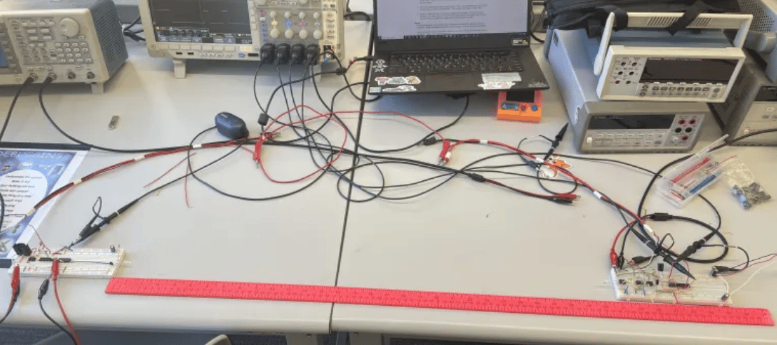
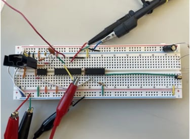
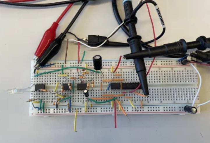
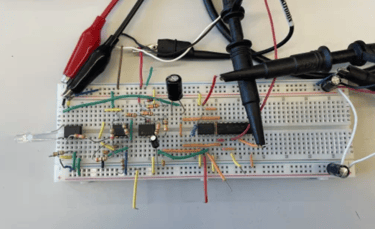
Breadboard Circuits
Transmitter Side:

Measurements and Analysis
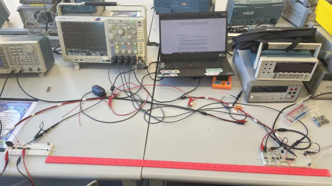
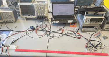
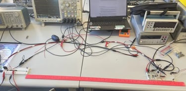
Picture of the entire setup, transmitter on the left and the receiver on the right
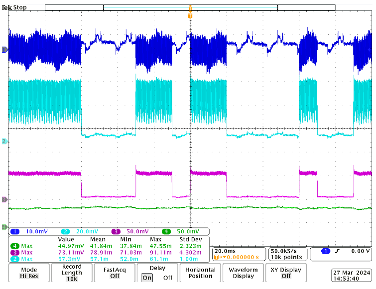
Below are waveform captures to verify the operation of the IR digital communication system. Each waveform is labeled 1 to 4 where the trace at the top is 1 while the trace at the bottom is 4. Following each waveform capture is a short description of the relationship and relevance of each trace, along with a schematic labeled with where the traces are measured.

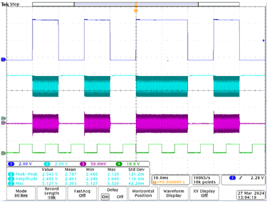
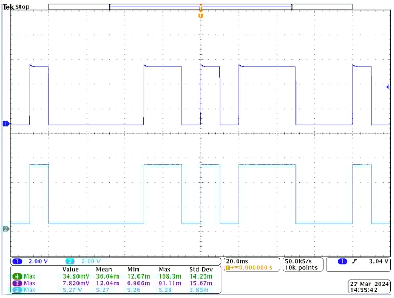
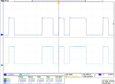
Oscilloscope capture of the relationship between PSG, LED anode voltage, and output of bandpass filter
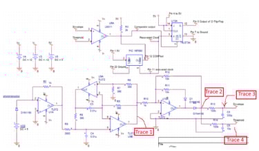
1 -Pseudorandom message sequence
2 - LED anode voltage
3 - output of bandpass filter
4 - transmitters bit clock
The pseudorandom message sequence is the data sequence being transmitted to the receiver circuit and stored. Thus, it is the first part of the transmitter circuit as this sequence now has to go through the process to be transmitted. The output of the LED anode voltage shows the carrier frequency in the LED as it oscillates between on and off when delivering a 1’s bit. This output verifies that not only is the LED being properly driven, but the overall shape of the signal being transmitted resembles that of the PSG which shows that the data is being sent correctly. The output of the bandpass filter shows that the DC offset value is eliminated and that the signal is properly received by the receiver breadboard. The shape of the waveform still resembles the PSG output so the bits are still properly there. The last trace shows the transmitter bit clock which shows that the bits of the PSG output are being generated at the correct frequency.
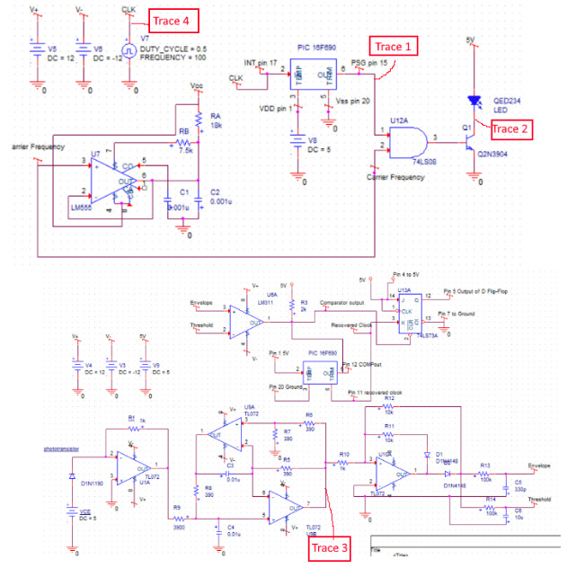
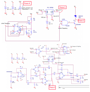
Trace locations for the waveform capture
Waveform capture of the relationship of the bandpass filter and half-wave rectifier with the envelope and threshold.
1 - modulated signal after bandpass filter
2 - rectified signal after a half-wave rectifier
3 - envelope
4 - threshold
The first trace is of the output of the bandpass filter as a carry-on from the previous waveform to show the outline of the PSG output. The second trace is the output of the half-wave rectifier to show that a large portion of the 40 kHz carrier frequency has been eliminated. Note: the above waveform was taken before a larger capacitor was switched out in the low-pass filter of the band-pass filter, so there is still a large portion of the carrier frequency present in this output. It should resemble the envelope more than the bandpass filter's output.
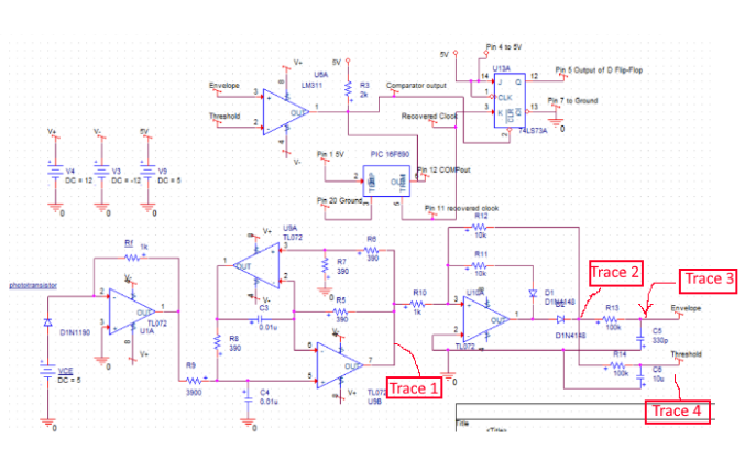
Trace locations for the waveform capture
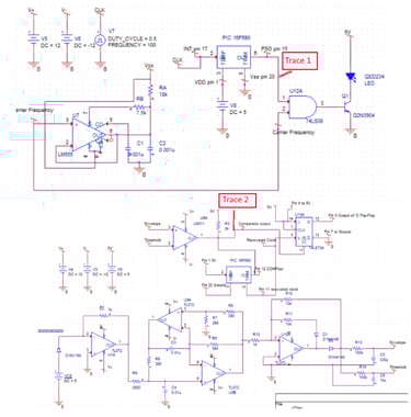
Waveform capture comparing the PSG output and comparator output
1 - PSG output
2 - comparator output
The first trace is to show the original pseudorandom data sequence, while the second trace is to show the successfully received sequence on the receiver breadboard. These two traces can be used to verify that all bits were transmitted properly and none were lost, as they should be exact copies of each other.
It can also be seen in the above waveforms that there is some noise. The above traces should be a lot smoother. The output of the second trace confirms that the data sequence is still not lost and is being filtered properly. The envelope's output verifies that the PSG output was successfully recovered, as it closely resembles the transmitted message sequence but has a bit of noise. The threshold output shows that its peak value is approximately half the value of the peak of the envelope, so when the envelope and threshold are inputs for the comparator in the next part of the circuit, the output of the comparator cleans up the signal nicely.

Trace locations for the waveform capture
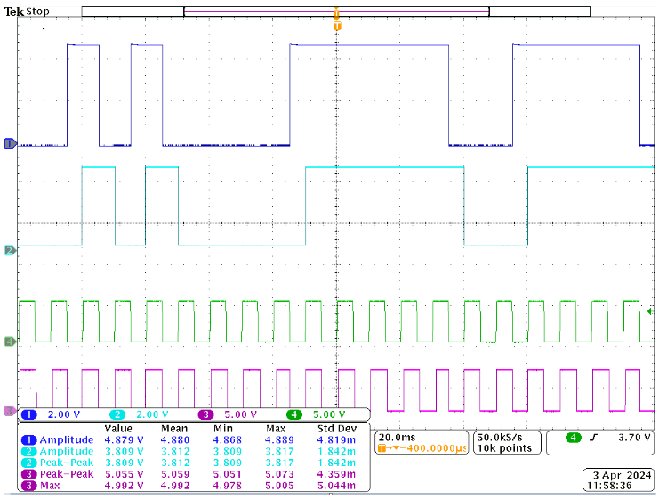
Waveform capture of PSG, D flip-flop output, and the bit clocks of the transmitter and receiver
1 - PSG output
2 - D flip-flop output
3 - transmitters bit clock
4 - receiver's bit clock
Trace locations for the waveform capture
The first trace is to show the original pseudorandom bit sequence sent from the transmitter breadboard. The second trace shows the signal stored on the receiver breadboard, which is an exact copy of the PSG output but is delayed by half a period due to the data being clocked in the D flip-flop. By verifying that the two traces look the same, it can be concluded that the IR digital communication system works. Trace 3 shows the transmitter's bit clock, while trace 4 shows the receiver’s recovered bit clock. These two traces show that the timing recovery system works correctly and the comparator’s output can be stored in the D flip-flop at the correct frequency.
IR LED Behavior
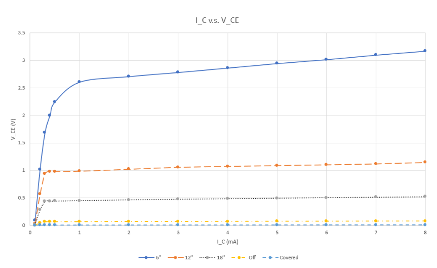
Characteristics of the phototransistors with distance and the relationship of current and voltage
The graph above depicts the various cases of IR LED and phototransistor separation by 6, 12, and 18 inches, along with LED off and LED covered. From 0 to 0.75V is the saturation region. At VCE=5V and the LED is off, the phototransistor produces 0.076mA of current, while when the LED is on and separated by 6 inches, the phototransistor produces 2.944mA of current.
Bandpass Filter Design
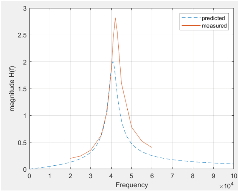
Plot of measured and predicted frequency response of the bandpass filter

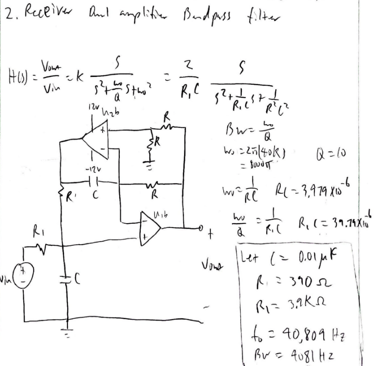
The above is a picture showing the calculation for the bandpass filter design, as well as a graph comparing the measured and predicted frequency response. The actual bandpass filter is shifted to the right of the frequency bands and has a broader passband, but it still passes the carrier frequency at 40 kHz.
Conclusion
The final IR signal transmitter and receiver work properly up to a distance of 32 inches. Data can be transmitted up to 3.9kHz bits/sec. With these conditions, the data sequence transmitted is perfectly received in the D Flip-Flop of the receiver circuit.
There were a few rough spots in the process of building all the subsystems. The voltage regulator we made worked well for the first half of the lab; however, when we were wiring up the envelope detector, the voltage regulator burnt out as we realized the wall adapter was sourcing 12VDC to the regulator instead of 9VDC. We rectified this by running it off the power supply instead. We also discovered that for the dual-amplifier bandpass subsystem we built, the capacitor value of the low-pass filter was too small, as there was still a large portion of the 40kHz carrier present when going into the envelope detector. We also messed up on a later part of the lab where we clocked the carrier oscillator with the frequency of the bit clock, not the 40kHz. Thus, the output of the bandpass filter was not the expected output.
While building the IR transmitter and receiver, we got to design and apply concepts about communication systems that we learned during the lecture, including how bit clocks are synchronized on the transmitter and receiver ends, and how a receiver cleans up and recovers the transmitted signal through the use of an envelope detector. We also saw how bit rate affected the probability of error through the eye diagram. Overall, the lab experience enhanced the learning experience through hands-on application and experimentation.
Project Overview
The goal of this project was to create an IR Digital communication system by transmitting a pseudorandom bit sequence between two breadboards at least a distance of 18 inches apart, with no loss or error in bits and only a slight time delay. To do this, we built an interface for phototransistors, a voltage regulator, a pseudorandom bit sequence generator, a Voltage Comparator using an LM311, a sampler using a D Flip-Flop, a Dual-Amplifier Bandpass Filter, a Carrier Oscillator, an Envelope detector, and finally a timing recovery system.
The transmitter breadboard contains the pseudorandom bit generator, along with the voltage regulator to provide a 5V power supply, a carrier oscillator to modulate the signal, and a phototransistor transmitter. With this board, the phototransistor will oscillate between on and off at the rate of the carrier oscillator when the pseudorandom bit generator's value is high and will remain on when the pseudorandom bit generator's value is low.
On the receiver side, the IR phototransistor receives the signal and passes it through a dual-amplifier bandpass filter, envelope detector, and comparator to clean up the signal. The received signal finally passes through the timing recovery system, where a PIC is programmed to recover the bit clock for the D Flip-Flop to store the transmitted signal.
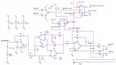
From the schematics above, two PIC devices are programmed to act as the pseudo-random bit generators and the timing recovery system.
Receiver Side:
Transmitter Side:
Receiver Side:
Transmitter Side:
Circuit Schematics
Circuit Block Diagram
System Block Diagram
Transmitter Side:
Receiver Side:
Receiver Side: